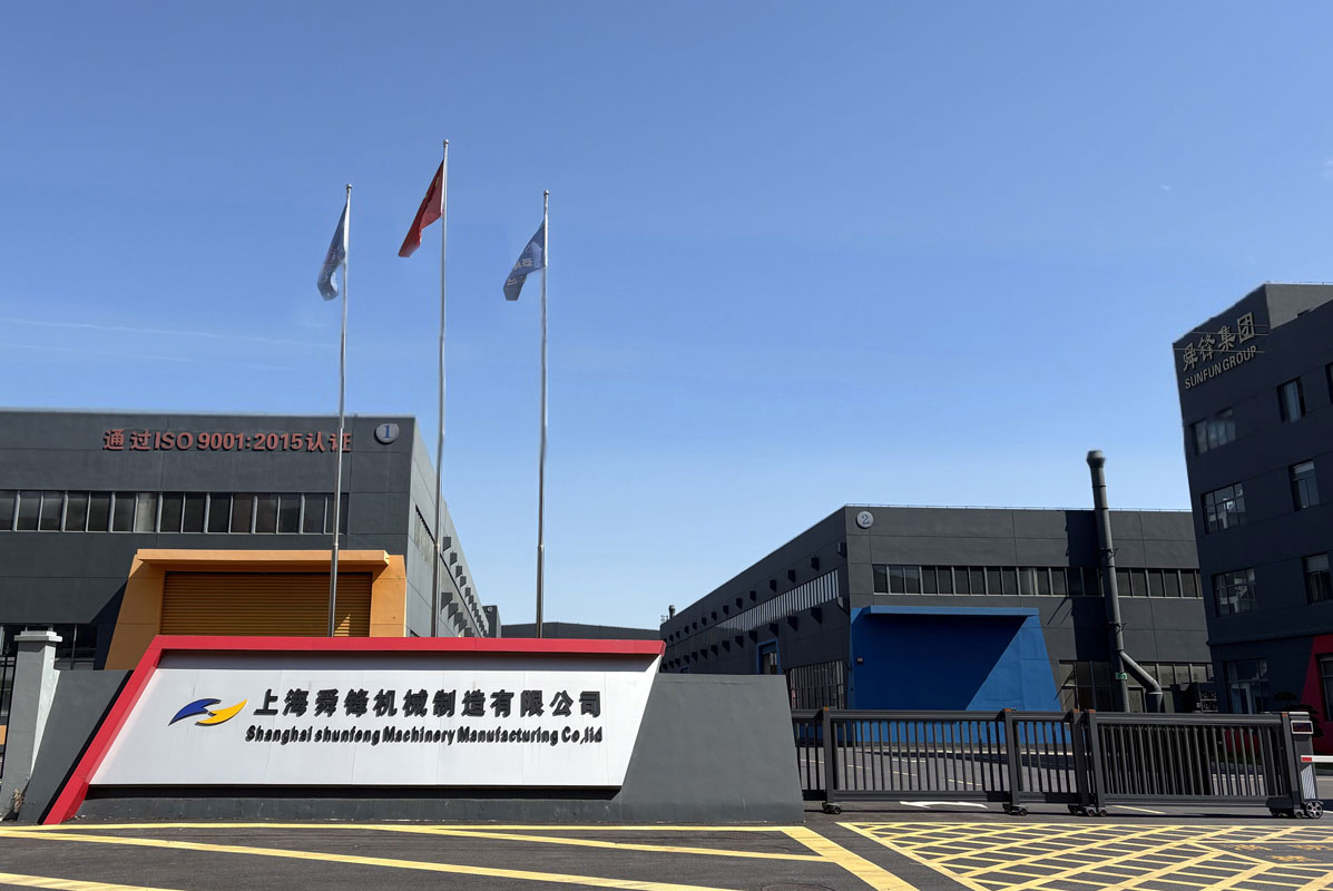


SUNFUN Group specializes in intelligent and sustainable industrial development. Driving quality advancement in manufacturing across China and the globe through technological innovation, we are committed to creating green value for a better human life.
We have deep expertise in smart energy and smart manufacturing, consistently achieving breakthroughs in precision production. Our capabilities range from 0.001-mm precision machining to the manufacture of components weighing from 0.1 grams to 150 tons. We maintain energy consumption within 0.1% and implement fully intelligent process management—all supported by four decades of specialized experience!
Innovation is the foundation of the growth of our group. We have built an open and collaborative innovation ecosystem, partnering with governments, enterprises, universities, and institutions to enable cooperative innovation and shared value, injecting sustained momentum into the industry.<br/>
As an accredited technology enterprise with its own institute and talent academy, SUNFUN has completed more than ten national-level R&D tasks and undertaken major projects commissioned by agencies such as the NDRC, MOST, and MIIT.
HJT equipment is the key equipment for producing HJT (Heterojunction with Intrinsic Thin layer) cells, mainly including cleaning and texturing equipment, PECVD equipment, PVD/RPD equipment, etc. HJT (intrinsic thin film heterojunction) cells are symmetrical double-sided cell structures, with N-type crystalline silicon in the middle, and then depositing intrinsic amorphous silicon thin films and P-type amorphous silicon thin films on the front to form a PN junction. On the back of the silicon wafer, intrinsic amorphous silicon thin films and N-type amorphous silicon thin films are also deposited in sequence to form a back surface field. Crystalline silicon, its crystalline form is similar to quartz, graphite and other materials, and its structure has high crystallinity, so it has high conductivity and photoelectric conversion efficiency. It creatively combines the advantages of crystalline silicon and amorphous silicon. HJT needs to deposit transparent conductive films (TCO) on both sides of the cell for conductivity, and then use screen printing technology to form double-sided electrodes. HJT technology has well solved the problem of high carrier recombination loss in the doping layer and substrate contact area of conventional cells.