Semiconductor Equipment (Focus on third-generation semiconductors) Industry knowledge
What are the most common failure modes in semiconductor deposition equipment?
The most common failure modes in semiconductor deposition equipment include particle contamination, gas delivery system failures, heater and temperature control issues, vacuum integrity loss, and plasma generation system degradation. These failures affect deposition uniformity, film quality, and process repeatability—leading to yield loss and equipment downtime. SUNFUN Group has been manufacturing precision components for semiconductor equipment since 1986, applying 0.001‑mm precision machining to produce parts that meet the demanding reliability requirements of advanced deposition tools.
Product Category 1: CVD Deposition Equipment
Definition and Positioning
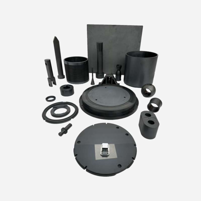
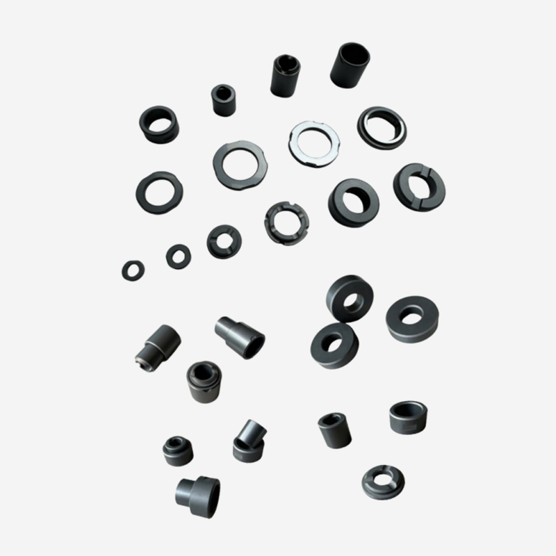
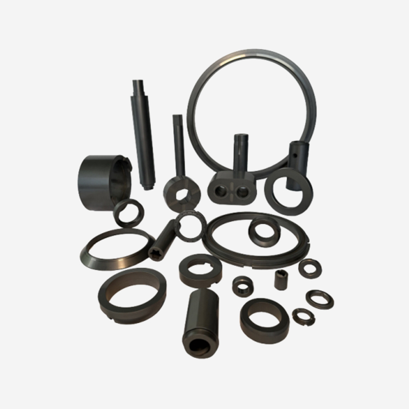
CVD deposition equipment is used to deposit thin films on semiconductor wafers through chemical reactions of precursor gases. The equipment includes reaction chambers, gas delivery systems, heating systems, and exhaust systems. SUNFUN Group manufactures precision components for CVD systems—including susceptors, gas distribution components, and vacuum system parts—that must withstand high temperatures and aggressive chemistries. As semiconductor equipment components, these parts support the reliability requirements of advanced deposition processes for third‑generation semiconductors.
Core Functions and Technical Features
CVD equipment functions by delivering precursor gases to a heated wafer surface, where chemical reactions deposit the desired film material. The critical subsystems—gas delivery, thermal control, and vacuum—must maintain precise, stable conditions to achieve consistent film quality. Gas delivery systems must maintain accurate flow control across a range of precursor chemistries. Heating systems must provide uniform temperature across the wafer surface. Vacuum systems must maintain the pressure conditions required for deposition.
Common failure modes in CVD equipment include gas line blockages from precursor condensation or particle accumulation, heater failure causing temperature non‑uniformity, thermocouple degradation affecting temperature measurement accuracy, and vacuum leak development affecting pressure control and process gas integrity. Component wear from thermal cycling and chemical exposure also contributes to failure. SUNFUN Group's precision components are manufactured with materials and tolerances that extend service life in CVD applications. These deposition equipment components support reliable operation through demanding production schedules.
Typical Application Scenarios
CVD deposition equipment is used in semiconductor fabrication for depositing dielectric films, conductor films, and semiconductor layers. Silicon nitride and silicon dioxide films are deposited for dielectric applications. Polysilicon and metal films are deposited for conductor applications. SiC and GaN layers are deposited for third‑generation semiconductor applications.
Differentiation from Other Deposition Methods
CVD equipment is distinguished from physical vapour deposition (PVD) methods by its use of chemical reactions for film formation, higher operating temperatures, and more complex gas handling systems. The failure modes reflect these differences—CVD systems are more susceptible to gas delivery and thermal control failures.
SUNFUN Group's Manufacturing Capabilities
SUNFUN Group's CVD component production applies precision machining and quality control appropriate for semiconductor applications. Our 0.001‑mm precision machining ensures that susceptors and gas distribution components meet dimensional requirements for consistent deposition. Through our open innovation ecosystem, established in partnership with governments, enterprises, universities, and institutions, we maintain knowledge of evolving CVD requirements for third‑generation semiconductors.
CVD Equipment Specifications
- Temperature range: 400‑1,200 °C
- Pressure range: mTorr to atmospheric
- Precursor gases: Various chemical precursors
- Film types: Dielectric, conductive, semiconductor
- Substrate materials: Silicon, SiC, GaN, sapphire
- Deposition uniformity: ±3‑5 % across wafer
Product Category 2: PVD Deposition Equipment
Definition and Positioning
PVD deposition equipment—including sputtering and evaporation systems—deposits thin films through physical processes, including ion bombardment and thermal evaporation. These systems are widely used for metal deposition, transparent conductive oxide deposition, and barrier layer formation. SUNFUN Group manufactures precision components for PVD equipment, including target holders, substrate carriers, and shielding components that must withstand plasma exposure and high vacuum conditions. These semiconductor equipment components support the reliability requirements of PVD deposition.
Core Functions and Technical Features
PVD equipment functions by generating a flux of material atoms or ions that deposit on the wafer surface. Sputtering systems use plasma to bombard a target, ejecting material atoms that travel to the wafer. Evaporation systems use thermal or electron beam heating to vaporise material, condensing on the wafer surface. The critical subsystems—plasma generation, vacuum, and wafer handling—must maintain stable conditions for consistent deposition.
Common failure modes in PVD equipment include cathode failure from target erosion and thermal stress, power supply degradation affecting plasma stability, cooling system failure causing overheating, particle generation from target wear or flaking, and vacuum integrity loss affecting deposition quality. SUNFUN Group's components are manufactured with wear‑resistant materials and precision tolerances that extend service life in PVD applications. These deposition equipment components support consistent film quality through demanding production schedules.
Typical Application Scenarios
PVD deposition equipment is used for metal deposition in semiconductor fabrication, TCO deposition for optoelectronics, and barrier layer formation. Aluminium and copper films are deposited for interconnect applications. ITO and zinc oxide are deposited for optoelectronic applications. Titanium nitride and tantalum nitride are deposited for barrier and adhesion applications.
Differentiation from CVD Equipment
PVD equipment is distinguished from CVD equipment by its physical deposition mechanism, lower operating temperatures, and higher sensitivity to target and source condition. Failure modes in PVD equipment are more closely related to target erosion and plasma generation, while CVD failure modes are more related to gas delivery and chemical precursor handling.
SUNFUN Group's Manufacturing Capabilities
SUNFUN Group's PVD component production applies precision machining and quality control appropriate for semiconductor applications. Our in‑house institute and talent academy provide technical expertise in component design for PVD applications. Our accredited technology enterprise status—demonstrated through national‑level R&D tasks and projects commissioned by the NDRC, MOST, and MIIT—supports quality systems for third‑generation semiconductors.
PVD Equipment Specifications
- Temperature range: Ambient – 500 °C
- Pressure range: 10⁻³‑10⁻⁷ mbar
- Target materials: Metals, alloys, oxides, nitrides
- Deposition rate: 10‑100 nm/minute
- Plasma power: 1‑20 kW
- Uniformity: ±3‑5 % across wafer
Product Category 3: ALD Deposition Equipment
Definition and Positioning
ALD deposition equipment enables atomic‑scale film deposition through sequential self‑limiting surface reactions. This precision deposition method is essential for advanced semiconductor devices requiring atomic‑level thickness control. SUNFUN Group manufactures precision components for ALD systems—including gas distribution manifolds, heated components, and sealing elements—that must maintain ultra‑clean conditions and high purity. These semiconductor equipment components support the precision requirements of ALD deposition for third‑generation semiconductors.
Core Functions and Technical Features
ALD equipment functions by delivering alternating precursor pulses to the wafer surface, with each pulse producing a self‑limiting surface reaction that deposits a monolayer of material. The critical subsystems—precursor delivery, temperature control, and purge gas handling—must operate with high precision and cleanliness to achieve atomic‑layer control. The process requires rapid switching between precursor and purge gases, with precise temperature control to maintain the surface reaction conditions.
Common failure modes in ALD equipment include precursor line contamination causing film quality issues, valve failure affecting pulse timing and sequence integrity, particulate contamination from precursor decomposition, and temperature control failure affecting reaction uniformity. SUNFUN Group's components are manufactured with the precision and cleanliness required for ALD applications. These deposition equipment components support atomic‑level film control in advanced semiconductor fabrication.
Typical Application Scenarios
ALD deposition equipment is used for high‑k dielectric deposition, metal gate electrode formation, and passivation layer deposition in advanced semiconductor devices. Al₂O₃ and HfO₂ are deposited for high‑k dielectric applications. TiN and TaN are deposited for metal gate and barrier applications.
Differentiation from Other Deposition Methods
ALD is distinguished from CVD and PVD methods by its self‑limiting surface reaction mechanism, which provides atomic‑layer thickness control. The deposition rate is lower than CVD and PVD methods, but the precision and conformality are superior. The failure modes reflect the precision requirements of ALD, with precursor delivery and valve reliability being critical factors.
SUNFUN Group's Manufacturing Capabilities
SUNFUN Group's ALD component production applies precision machining and cleanliness standards appropriate for advanced semiconductor applications. Through our open innovation ecosystem, we maintain knowledge of evolving ALD requirements for third‑generation semiconductors.
Key Specifications Comparison
| Parameter |
CVD |
PVD |
ALD |
| Deposition mechanism |
Chemical reaction |
Physical transport |
Self‑limiting surface reaction |
| Deposition rate |
Moderate |
High |
Low |
| Thickness control |
Ångström to nanometre |
Nanometre |
Atomic layer |
| Common failure modes |
Gas delivery, thermal |
Target erosion, plasma |
Precursor, valve |
| Applications |
Dielectric, semiconductor |
Metal, TCO |
High‑k, gate, passivation |
The most common failure modes in semiconductor deposition equipment include gas delivery failures, temperature control issues, vacuum integrity loss, and component degradation from process exposure. SUNFUN Group manufactures precision components for all types of deposition equipment—CVD, PVD, and ALD—applying precision machining and quality control developed over four decades of experience. Our 0.001‑mm precision machining ensures that deposition equipment components meet dimensional requirements for reliable, consistent performance. Through our in‑house institute, talent academy, and open innovation ecosystem—established in partnership with governments, enterprises, universities, and institutions—SUNFUN Group maintains the technical expertise required for semiconductor equipment that supports the demanding requirements of third‑generation semiconductor manufacturing.
Frequently Asked Questions
Q1: What is the most common cause of failure in CVD equipment?
The most common cause of failure in CVD equipment is gas delivery system issues—including precursor line blockages, flow control failures, and valve problems. These issues can affect deposition uniformity and film quality. Semiconductor equipment used for CVD requires regular maintenance of gas delivery systems to prevent failure.
Q2: Why is target erosion a significant failure mode in PVD equipment?
Target erosion in PVD equipment leads to film thickness non‑uniformity, increased particle generation, and eventual target failure. The erosion pattern affects the deposition flux distribution across the wafer, requiring periodic target replacement. Deposition equipment in PVD applications requires careful target management for consistent performance.
Q3: What makes ALD equipment particularly sensitive to component quality?
ALD equipment's atomic‑level thickness control makes it particularly sensitive to precursor delivery timing, valve performance, and temperature uniformity. Small variations in these parameters can affect film thickness at the atomic scale. Third‑generation semiconductors fabricated with ALD require extremely precise component quality.
Q4: What quality controls apply to SUNFUN Group's semiconductor equipment component manufacturing?
SUNFUN Group applies material certification, dimensional verification, surface finish measurement, and cleanliness inspection to all semiconductor component production. Our accredited technology enterprise status supports comprehensive quality systems for semiconductor equipment, ensuring consistent component quality and reliable processing performance.


 English
 日本語
日本語
 عربى
عربى
 中文简体
中文简体