Why is pan‑semiconductors equipment critical for compound semiconductor manufacturing?
Pan‑semiconductors equipment is critical for compound semiconductor manufacturing because it enables the precision processing of materials such as silicon carbide (SiC), gallium nitride (GaN), and other wide‑bandgap semiconductors—materials that are essential for power electronics, 5G communications, and electric vehicle applications. These advanced materials require specialised handling and processing equipment capable of operating at high temperatures, maintaining ultra‑clean conditions, and delivering micron‑level precision across large substrate sizes. SUNFUN Group has been manufacturing precision components and equipment since 1986, applying 0.001‑mm machining capabilities to support the demanding requirements of compound semiconductor production.
Product Category 1: SiC Substrate Processing Equipment
Definition and Positioning
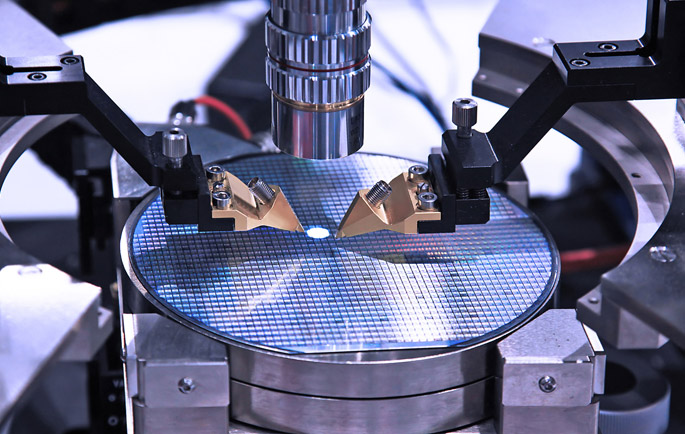
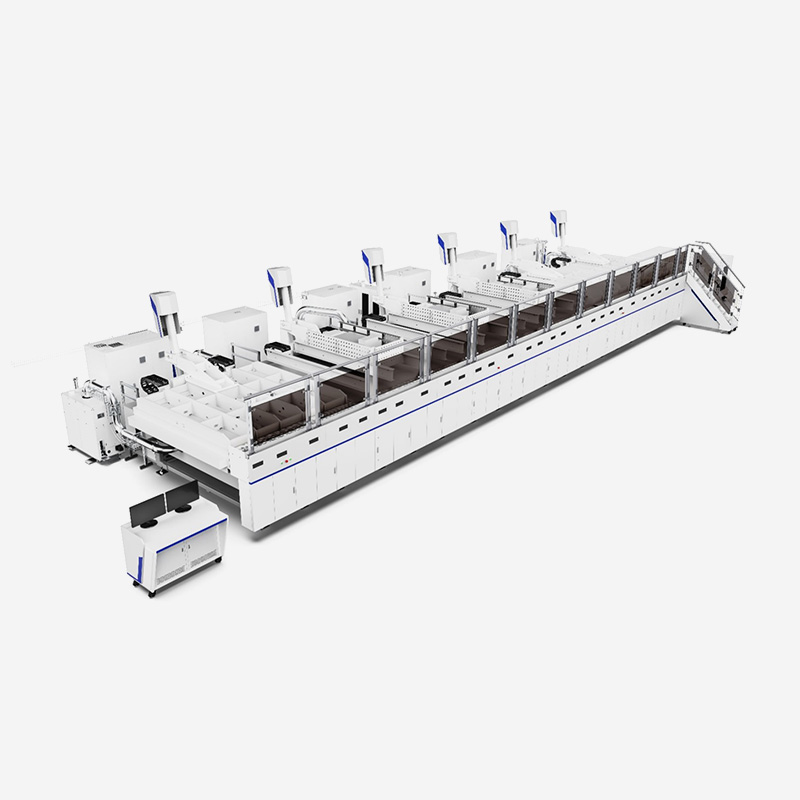
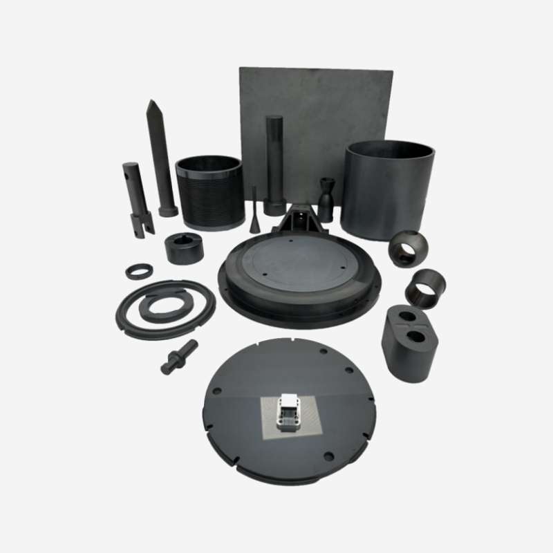
SiC substrate processing equipment encompasses the specialised machinery required to convert raw silicon carbide crystals into polished wafers ready for epitaxial growth and device fabrication. This includes slicing, grinding, lapping, and polishing systems designed specifically for the hardness and brittleness of SiC—one of the hardest commercially used materials. SUNFUN Group manufactures precision components for SiC processing equipment, including spindles, workholding fixtures, and precision mounting surfaces. As pan‑semiconductors equipment & components, these parts must meet the exacting requirements of SiC wafer processing.
Core Functions and Technical Features
SiC substrate processing equipment functions through the application of diamond‑based abrasives and specialised machining techniques to address the unique properties of silicon carbide. Slicing equipment uses diamond wire or annular saws to cut ingots into wafers. Grinding equipment uses diamond wheels to flatten wafers and achieve initial thickness. Lapping equipment uses diamond slurries with cast‑iron plates to achieve flatness and surface finish. Polishing equipment uses finer abrasives to achieve the surface quality required for epitaxial growth.
The design of SiC processing equipment emphasises process stability and precision. Spindles must maintain accurate rotation with minimal runout to achieve consistent material removal. Workholding must accommodate the rigidity of SiC while maintaining orientation accuracy. SUNFUN Group's components are manufactured with the precision required for consistent SiC processing. These pan‑semiconductors equipment & components are essential for achieving the substrate quality required for compound semiconductor devices.
Typical Application Scenarios
SiC substrate processing equipment is used in facilities that manufacture SiC wafers for power electronics and RF devices. Substrate suppliers operate slicing, grinding, and polishing lines to produce wafers for device manufacturers. Device manufacturers may also operate processing equipment to qualify incoming wafers and perform rework operations.
Differentiation from Silicon Processing Equipment
SiC processing equipment is distinguished from silicon processing equipment by its use of diamond abrasives, higher force requirements, and slower processing rates. SiC is substantially harder than silicon, requiring specialised tools and techniques. The processing equipment must also operate in cleaner environments and maintain tighter process control due to the higher value of SiC wafers.
SUNFUN Group's Manufacturing Capabilities
SUNFUN Group's SiC processing equipment component production applies precision machining and quality control appropriate for semiconductor applications. Our 0.001‑mm precision machining ensures that spindles and fixtures meet dimensional requirements for consistent wafer processing. Through our open innovation ecosystem, established in partnership with governments, enterprises, universities, and institutions, we maintain knowledge of evolving SiC processing requirements for pan‑semiconductors equipment & components.
SiC Processing Equipment Specifications
- Wafer sizes: 100 mm, 150 mm, 200 mm
- Surface finish: Ra ≤ 0.5 nm (polished)
- Flatness: ≤ 5 µm TTV
- Thickness range: 200 µm – 500 µm
- Materials processed: 4H‑SiC, 6H‑SiC
- Process environment: Cleanroom (Class 100)
Product Category 2: GaN Processing and Deposition Equipment
Definition and Positioning
GaN processing and deposition equipment is used to fabricate gallium nitride devices on substrates such as SiC, sapphire, and silicon. This equipment includes metal‑organic chemical vapour deposition (MOCVD) systems, molecular beam epitaxy (MBE) systems, and associated processing tools. SUNFUN Group manufactures precision components for GaN processing equipment, including susceptors, gas distribution components, and vacuum system components. These pan‑semiconductors equipment & components support the fabrication of GaN‑based optoelectronics and power devices.
Core Functions and Technical Features
GaN processing equipment functions through the controlled deposition and processing of gallium nitride and related materials. MOCVD systems deposit GaN layers on substrates by reacting metal‑organic precursors and ammonia at elevated temperatures. MBE systems deposit GaN through molecular beam epitaxy under ultra‑high vacuum. Processing equipment includes etching, cleaning, and annealing tools that prepare surfaces and define device structures.
The design of GaN processing equipment emphasises temperature uniformity, gas distribution control, and contamination management. Susceptors must maintain uniform temperature across wafer surfaces to achieve consistent deposition. Gas distribution components must deliver precursors uniformly to the wafer surface. Vacuum components must maintain clean, controlled environments. SUNFUN Group's components are manufactured with precision to meet these requirements. These pan‑semiconductors equipment & components are essential for GaN device fabrication.
Typical Application Scenarios
GaN processing equipment is used in facilities that manufacture optoelectronics and power devices. LED manufacturers use MOCVD for GaN‑based light‑emitting diode structures. Power device manufacturers use MBE and MOCVD for GaN high‑electron‑mobility transistors. RF device manufacturers use GaN processing for high‑frequency, high‑power applications.
Differentiation from SiC Processing Equipment
GaN processing equipment differs from SiC processing equipment in its focus on deposition and epitaxial growth, rather than substrate machining. GaN processing requires clean, ultra‑high vacuum or controlled atmosphere environments, while SiC processing focuses on mechanical material removal.
SUNFUN Group's Manufacturing Capabilities
SUNFUN Group's GaN processing component production applies precision machining and quality control appropriate for semiconductor deposition and processing applications. Our in‑house institute and talent academy provide technical expertise in component design for semiconductor applications. Our accredited technology enterprise status—demonstrated through national‑level R&D tasks and projects commissioned by the NDRC, MOST, and MIIT—supports quality systems for pan‑semiconductors equipment & components.
GaN Equipment Specifications
- Temperature range: Up to 1,200 °C (MOCVD)
- Pressure range: UHV to atmospheric
- Wafer sizes: 100 mm, 150 mm, 200 mm
- Deposition rate: 0.1 – 5 µm/hour
- Uniformity: ±2 % across wafer
- Process environment: Cleanroom (Class 10)
Product Category 3: Advanced Semiconductor Vacuum Components
Definition and Positioning
Advanced semiconductor vacuum components are essential for the compound semiconductor manufacturing environment, where many processes require UHV conditions and extremely clean surfaces. These components include vacuum chambers, valves, pumping systems, and sealing elements designed for the demanding requirements of SiC and GaN processing. SUNFUN Group manufactures vacuum components that support compound semiconductor manufacturing, applying precision machining to produce parts that maintain vacuum integrity and cleanliness. These pan‑semiconductors equipment & components ensure the production environment required for compound semiconductor device fabrication.
Core Functions and Technical Features
Advanced semiconductor vacuum components function to create and maintain the clean, controlled environments required for compound semiconductor processing. Vacuum chambers provide containment for high‑temperature and UHV processes. Valves enable isolation and process gas control. Pumping systems achieve the required pressure levels. Sealing elements maintain vacuum integrity through bakeout cycles and thermal cycling.
The design of advanced semiconductor vacuum components emphasises cleanability, low outgassing, and compatibility with aggressive process gases. Chambers are manufactured from stainless steel with electropolished internal surfaces. Valves incorporate metal sealing for high‑temperature bakeout compatibility. SUNFUN Group's vacuum components are manufactured with the precision and surface finish required for compound semiconductor applications. These pan‑semiconductors equipment & components support the clean, controlled environments essential for compound semiconductor fabrication.
Typical Application Scenarios
Advanced semiconductor vacuum components are used in all compound semiconductor processing equipment. MOCVD and MBE systems require UHV‑compatible components. Etching and deposition tools require vacuum components that maintain cleanliness and process integrity.
Differentiation from Standard Vacuum Components
Advanced semiconductor vacuum components are distinguished from standard components by their material selection, surface finish, and cleanliness requirements. Compound semiconductor processing requires the highest levels of cleanliness and process integrity, driving tighter specifications for vacuum components.
SUNFUN Group's Manufacturing Capabilities
SUNFUN Group manufactures advanced semiconductor vacuum components with the precision and surface quality required for compound semiconductor applications. Through our open innovation ecosystem, we maintain knowledge of evolving compound semiconductor requirements for pan‑semiconductors equipment & components.
Key Specifications Comparison
| Parameter |
SiC Processing |
GaN Processing |
Vacuum Components |
| Primary function |
Substrate preparation |
Deposition & processing |
Environment control |
| Environment |
Cleanroom |
UHV / controlled atmosphere |
UHV to rough vacuum |
| Temperature range |
Ambient – 200 °C |
Up to 1,200 °C |
Ambient – 450 °C |
| Critical tolerances |
Sub‑micron flatness |
Temperature uniformity |
Surface finish & leak rate |
| Key materials |
SiC, diamond, stainless steel |
Stainless steel, quartz, graphite |
Stainless steel, copper, elastomer |
Pan‑semiconductors equipment is critical for compound semiconductor manufacturing because it enables the precision processing of wide‑bandgap materials, supports advanced deposition and processing techniques, and maintains the clean, controlled environments required for device fabrication. SUNFUN Group manufactures precision components for pan‑semiconductors equipment across the full spectrum of compound semiconductor applications—from SiC substrate processing to GaN deposition and advanced vacuum systems. Our 0.001‑mm precision machining ensures that components meet dimensional requirements for consistent processing and device quality. Through our in‑house institute, talent academy, and open innovation ecosystem—established in partnership with governments, enterprises, universities, and institutions—SUNFUN Group maintains the technical expertise required for pan‑semiconductors equipment & components that support the demanding requirements of compound semiconductor manufacturing.
Frequently Asked Questions
Q1: What is the difference between pan‑semiconductors and conventional semiconductor equipment?
Pan‑semiconductors equipment is specifically designed for processing compound semiconductor materials such as SiC, GaN, and other wide‑bandgap materials. Conventional equipment is primarily designed for silicon processing. Pan‑semiconductors equipment addresses the higher temperatures, more aggressive chemistries, and harder materials associated with compound semiconductor manufacturing. Pan‑semiconductors equipment & components must meet these more demanding requirements.
Q2: Why is diamond used in SiC processing equipment?
Diamond is used because SiC is one of the hardest commercially used materials—silicon carbide abrasives would not effectively process SiC material. Diamond abrasives, including diamond wheels and diamond slurries, are required for processing SiC ingots and wafers. Pan‑semiconductors equipment & components must incorporate diamond‑based tools for SiC processing.
Q3: What temperature capabilities are required for GaN processing equipment?
GaN MOCVD systems require operating temperatures up to 1,200 °C to achieve the chemical reactions required for GaN deposition. Equipment must maintain temperature uniformity across wafer surfaces and accommodate thermal cycling. Pan‑semiconductors equipment & components for GaN processing must be designed for high‑temperature operation.
Q4: What quality controls apply to SUNFUN Group's pan‑semiconductors component manufacturing?
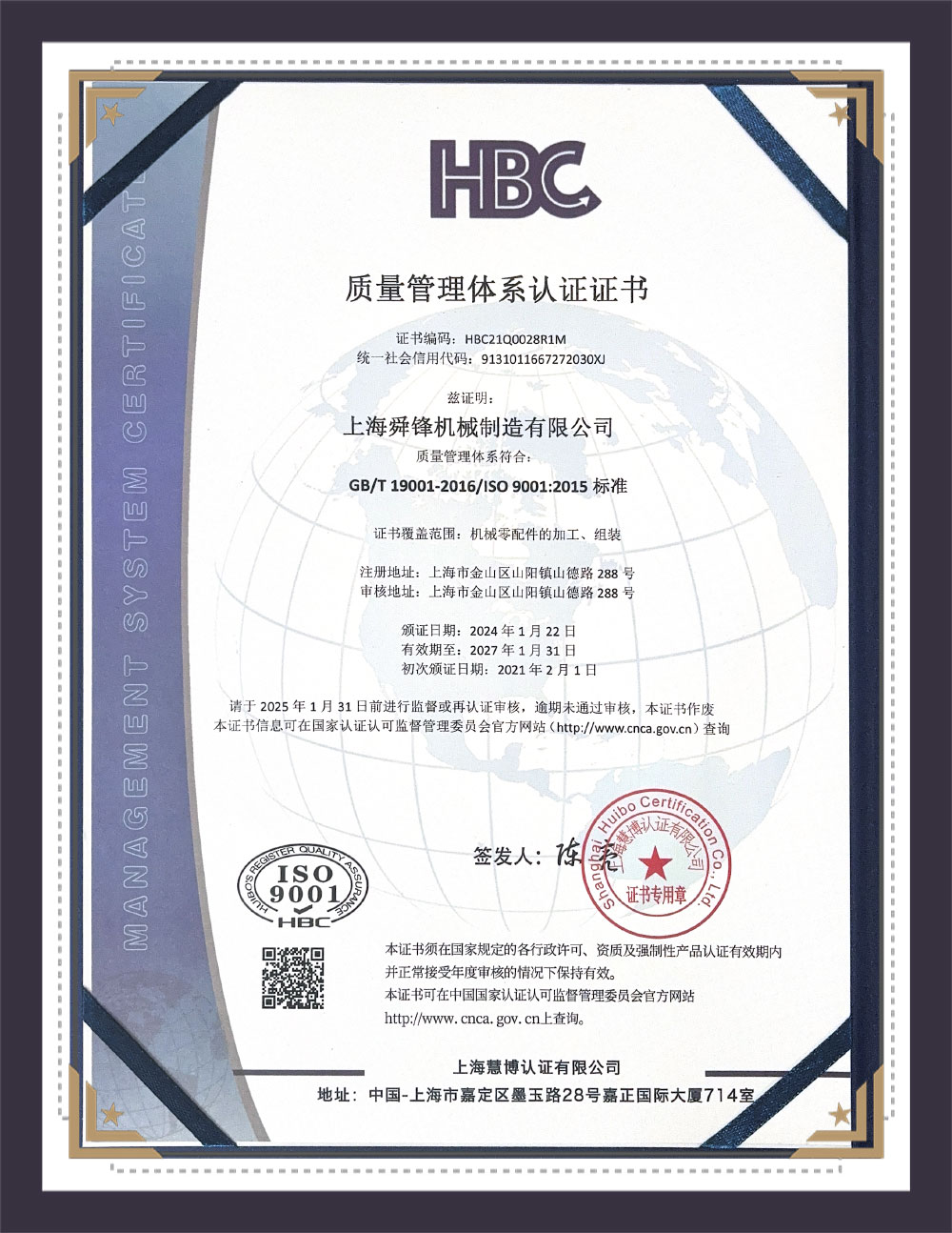
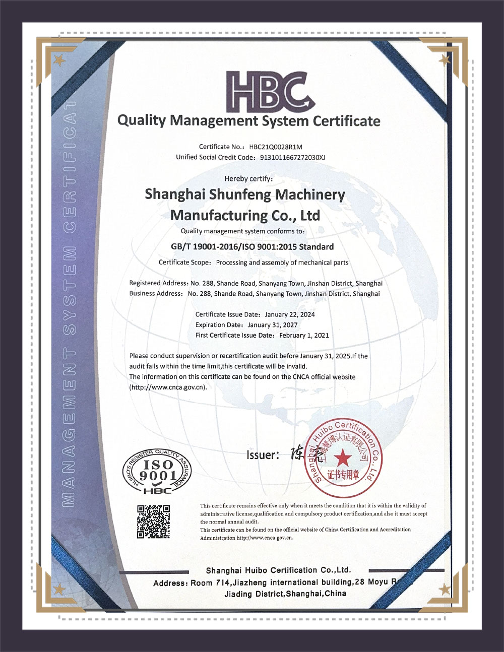
SUNFUN Group applies material certification, dimensional verification, surface finish measurement, and cleanliness inspection to all pan‑semiconductors component production. Our accredited technology enterprise status supports comprehensive quality systems for pan‑semiconductors equipment & components, ensuring consistent component quality and reliable semiconductor processing performance.


 English
 日本語
日本語
 عربى
عربى
 中文简体
中文简体