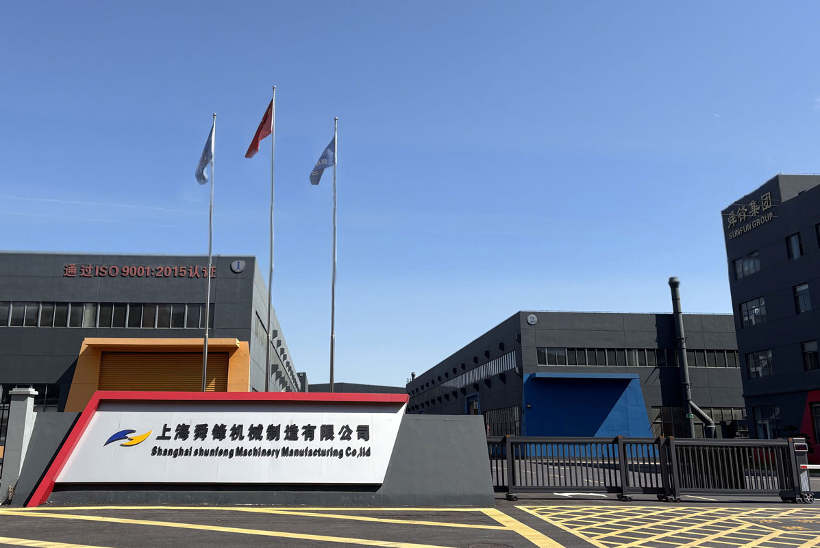
SUNFUN Group specializes in intelligent and sustainable industrial development. Driving quality advancement in manufacturing across China and the globe through technological innovation, we are committed to creating green value for a better human life.
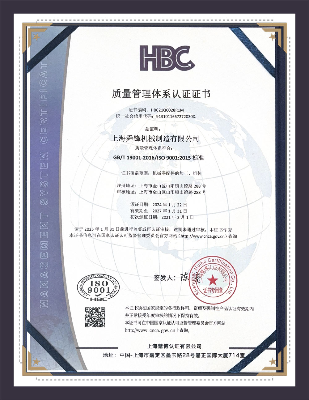
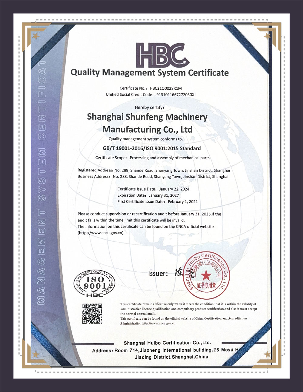
We have deep expertise in smart energy and smart manufacturing, consistently achieving breakthroughs in precision production. Our capabilities range from 0.001-mm precision machining to the manufacture of components weighing from 0.1 grams to 150 tons. We maintain energy consumption within 0.1% and implement fully intelligent process management—all supported by four decades of specialized experience!
Innovation is the foundation of the growth of our group. We have built an open and collaborative innovation ecosystem, partnering with governments, enterprises, universities, and institutions to enable cooperative innovation and shared value, injecting sustained momentum into the industry.<br/>
As an accredited technology enterprise with its own institute and talent academy, SUNFUN has completed more than ten national-level R&D tasks and undertaken major projects commissioned by agencies such as the NDRC, MOST, and MIIT.
This series of equipment adopts the combination of metal mode sputtering technology and a high-reactivity plasma source. The load-lock chamber is equipped with a manipulator to automatically transfer the substrate. The uniformity in mass production is less than 1%, realizing high-quality production.ffi
Patented RF-ICP/CCP ion source has the characteristics of a wide working range, balanced energy, high ionization rate, high stable working efficiency, and low energy consumption. It can clean the substrate and auxiliary coating to improve the quality of the film. The equipment is convenient and flexible. In large-scale production, it can simply and quickly switch the process and substrate, double rotating cylindrical cathode, stable discharge, multiple pairs of DC/Mf magnetron cathodes, support different materials, online adjustment of cathode magnetic field, high utilization rate of target, and improve film uniformity. Advanced on-site process control technology, the combination of plasma monitoring and broadband optical monitoring, provides excellent optical performance and improves output.
It is widely used to coat high-precision optical films on 2D/2.5D/ 3D substrates such as glass, plastic, and metal. It can deposit UV/ IR cut-off filter, band-pass filter, RGB filter, lidar, AR, hard AR film, hard film (Si3N4 or DLC), HR film, AS/ AF film, dielectric film(Ta2O5, Nb2O5, SiO2, Al2O3, TiO2, SiN, SiON), transparent conductive film (ITO), metal film (tantalum, titanium, aluminum, chromium, copper), decorative films (CrN, CrON), semiconductors (amorphous silicon, silicon), etc.