What is the role of power device processing equipment in electric vehicle manufacturing?
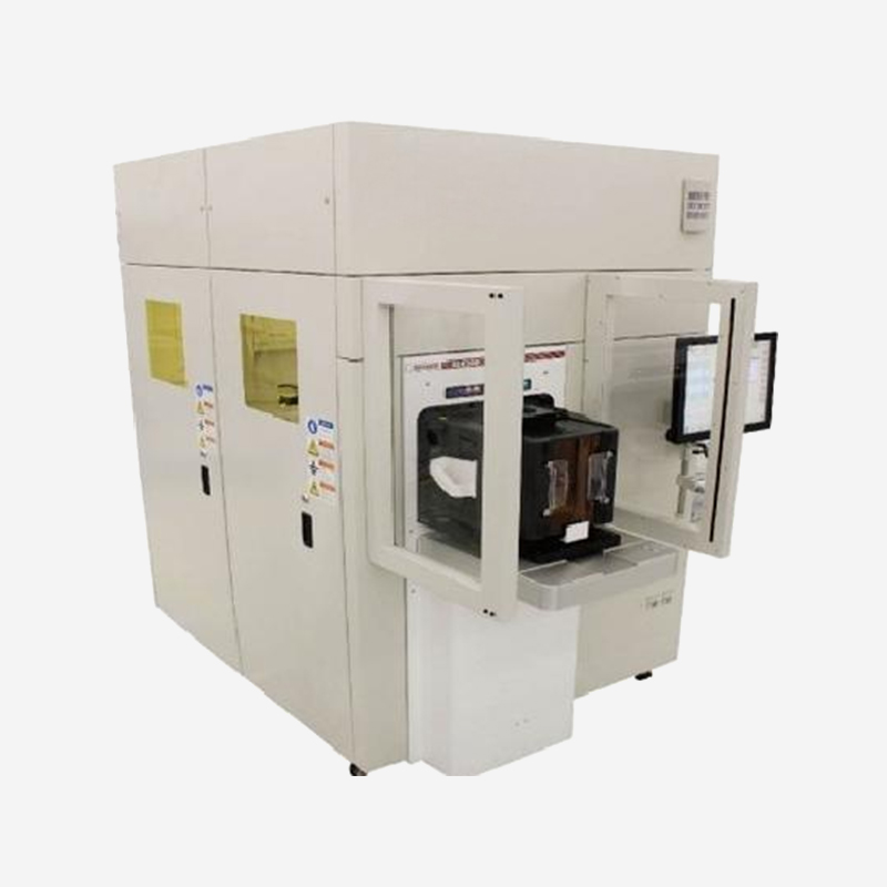
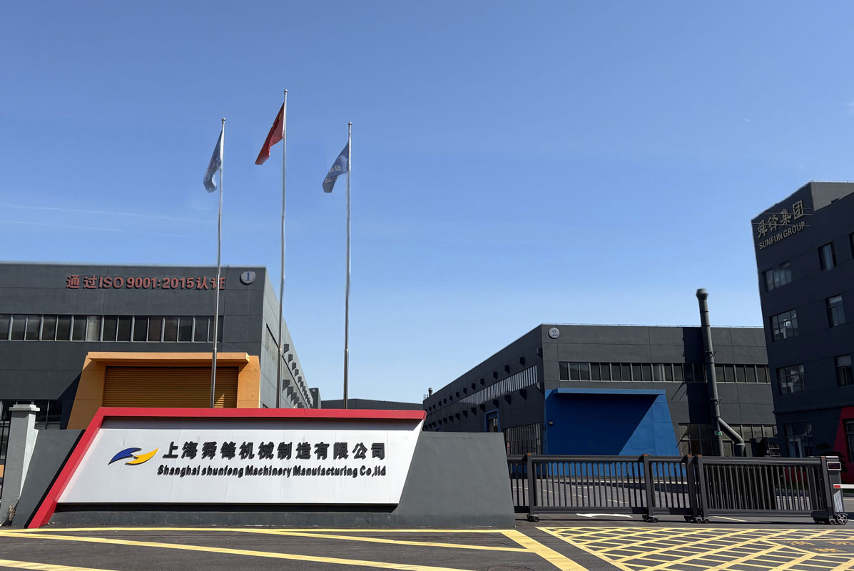
Power device processing equipment plays a critical role in electric vehicle manufacturing by enabling the production of silicon carbide (SiC) and other wide‑bandgap semiconductor devices that are essential for efficient power conversion in EV traction inverters, onboard chargers, and DC‑DC converters. This equipment transforms raw SiC substrates into high‑performance power devices that deliver superior efficiency, higher operating temperatures, and faster switching speeds compared to conventional silicon‑based power electronics. SUNFUN Group has been manufacturing precision components for power device processing equipment since 1986, applying 0.001‑mm precision machining to support the demanding requirements of SiC device fabrication.
Product Category 1: SiC Substrate Preparation Equipment
Definition and Positioning
SiC substrate preparation equipment encompasses the machinery required to prepare high‑quality SiC wafers for device fabrication—including slicing, grinding, lapping, and polishing systems. This equipment is critical for EV power device manufacturing because the substrate quality directly affects the performance, reliability, and yield of the final power devices. SUNFUN Group manufactures precision components for substrate preparation equipment, including spindles, workholding systems, and precision mounting surfaces. As silicon carbide wafer processing equipment, these components support the demanding requirements of SiC substrate fabrication.
Core Functions and Technical Features
SiC substrate preparation equipment functions through multi‑step processing that converts raw SiC ingots into polished wafers ready for epitaxial growth and device fabrication. Slicing equipment—typically using diamond wire or annular saws—cuts SiC ingots into wafers with minimal kerf loss. Grinding equipment flattens wafers and achieves initial thickness control. Lapping equipment uses diamond slurries to achieve flatness and remove subsurface damage. Polishing equipment uses finer diamond abrasives to achieve the surface quality required for epitaxial growth and device fabrication.
The design of SiC substrate preparation equipment addresses the unique challenges of SiC processing—including extreme hardness, brittleness, and high value of the material. Equipment must provide precise control of processing parameters and maintain stable conditions through extended processing cycles. SUNFUN Group's precision components are manufactured to tolerances that support consistent substrate quality. These SiC substrate processing equipment components are essential for achieving the substrate quality required for high‑performance EV power devices.
Typical Application Scenarios
SiC substrate preparation equipment is used in facilities that manufacture SiC wafers for power device applications—including EV traction inverters, onboard chargers, and renewable energy systems. Wafer suppliers operate preparation equipment to produce wafers for device manufacturers. Device manufacturers may also operate preparation equipment for wafer qualification and rework.
Differentiation from Silicon Wafer Equipment
SiC substrate preparation equipment is distinguished from silicon wafer equipment by its use of diamond abrasives, higher processing force requirements, and more stringent process control. SiC is substantially harder than silicon, requiring specialised tools and longer processing times.
SUNFUN Group's Manufacturing Capabilities
SUNFUN Group's substrate preparation component production applies precision machining and quality control appropriate for semiconductor applications. Our 0.001‑mm precision machining ensures that spindles and workholding meet dimensional requirements for consistent substrate processing. Through our open innovation ecosystem, established in partnership with governments, enterprises, universities, and institutions, we maintain knowledge of evolving substrate processing requirements for semiconductor wafer processing equipment.
Substrate Preparation Specifications
- Wafer sizes: 100 mm, 150 mm, 200 mm
- Surface finish: Ra ≤ 0.5 nm (polished)
- Flatness: ≤ 5 µm TTV
- Thickness range: 200‑500 µm
- Process environment: Cleanroom
- Yield target: ≥ 90 %
Product Category 2: SiC Epitaxial Growth Equipment
Definition and Positioning
SiC epitaxial growth equipment—primarily chemical vapour deposition (CVD) and sublimation systems—deposits high‑quality epitaxial layers on SiC substrates, creating the device active region and drift layer structures required for power device performance. This equipment is critical for EV power device manufacturing because epitaxial layer quality determines the voltage rating, on‑resistance, and switching characteristics of the final device. SUNFUN Group manufactures precision components for epitaxial growth equipment—including susceptors, gas distribution systems, and heating elements—that must withstand the extreme temperatures and chemical environments of SiC epitaxy. These power device processing equipment components support the demanding requirements of SiC device fabrication.
Core Functions and Technical Features
SiC epitaxial growth equipment functions by depositing high‑purity SiC layers on substrate wafers through controlled chemical reactions at elevated temperatures. CVD systems deliver precursor gases—including silane and propane—to heated wafer surfaces, where reactions deposit SiC epitaxial layers. Sublimation systems use physical vapour transport for SiC epitaxy. The critical subsystems—temperature control, gas delivery, and chamber environment—must maintain precise, stable conditions to achieve the layer quality required for power device performance.
The design of SiC epitaxial growth equipment emphasises temperature uniformity, contamination control, and process repeatability. Susceptors must maintain uniform temperature across wafer surfaces to achieve consistent epitaxial thickness and doping profiles. Gas distribution systems must deliver precursor gases uniformly to the wafer surface. Vacuum and inert gas systems must maintain clean, controlled environments. SUNFUN Group's components are manufactured with the precision required for SiC epitaxy. These silicon carbide wafer processing equipment components are essential for achieving the epitaxial layer quality required for EV power devices.
Typical Application Scenarios
SiC epitaxial growth equipment is used in facilities that manufacture SiC power devices for EV applications. Device manufacturers operate epitaxial systems to produce wafers for device fabrication. Wafer suppliers may also operate epitaxial equipment to provide value‑added products to device manufacturers.
Differentiation from Silicon Epitaxy Equipment
SiC epitaxy equipment is distinguished from silicon epitaxy equipment by its higher operating temperatures (up to 1,600 °C), more aggressive process chemistries, and more stringent contamination control requirements. SiC epitaxy equipment must also handle the challenges of SiC substrate preparation and handling.
SUNFUN Group's Manufacturing Capabilities
SUNFUN Group's epitaxial equipment component production applies precision machining and quality control appropriate for high‑temperature semiconductor applications. Our in‑house institute and talent academy provide technical expertise in component design for SiC epitaxy. Our accredited technology enterprise status—demonstrated through national‑level R&D tasks and projects commissioned by the NDRC, MOST, and MIIT—supports quality systems for SiC substrate processing equipment.
Epitaxial Equipment Specifications
- Temperature: Up to 1,600 °C
- Pressure: 10‑1,000 mbar
- Wafer sizes: 100‑200 mm
- Growth rate: 5‑30 µm/hour
- Doping control: ±5 %
- Process environment: UHV or inert gas
Product Category 3: SiC Device Processing Equipment
Definition and Positioning
SiC device processing equipment includes ion implantation, annealing, etching, and metallisation systems that fabricate power device structures on SiC epitaxial wafers. This equipment is critical for EV power device manufacturing because it defines the device electrical characteristics—including breakdown voltage, on‑resistance, and switching speed. SUNFUN Group manufactures precision components for device processing equipment, including ion source components, heated stages, and process chamber components. These power device processing equipment components support the demanding requirements of SiC device fabrication.
Core Functions and Technical Features
SiC device processing equipment functions through precision fabrication processes that create device structures on SiC epitaxial wafers. Ion implantation equipment dopes specific areas of the device with controlled doping profiles. Annealing equipment activates implanted dopants and repairs process damage at high temperatures. Etching equipment defines device geometries with high precision and sidewall quality. Metallisation equipment forms device contacts with low contact resistance.
The design of SiC device processing equipment emphasises process precision, contamination control, and throughput. Implantation equipment must achieve precise depth and concentration control for consistent device performance. Annealing equipment must provide uniform temperature distribution at high temperatures. Etching equipment must achieve high‑quality sidewalls with minimal damage. SUNFUN Group's components are manufactured with precision that supports consistent device fabrication. These semiconductor wafer processing equipment components are essential for achieving the device characteristics required for EV power devices.
Typical Application Scenarios
SiC device processing equipment is used in facilities that manufacture SiC power devices for EV applications—including MOSFETs, Schottky diodes, and IGBTs. Device manufacturers operate processing equipment for device fabrication. Foundries may also provide device processing services to power device companies.
Differentiation from Silicon Device Equipment
SiC device processing equipment is distinguished from silicon device equipment by its higher processing temperatures, more aggressive process chemistries, and more challenging handling requirements. SiC processing also requires tighter contamination control due to the higher sensitivity of SiC devices to impurities.
SUNFUN Group's Manufacturing Capabilities
SUNFUN Group manufactures components for SiC device processing equipment with the precision required for power device applications. Through our open innovation ecosystem, we maintain knowledge of evolving device processing requirements for silicon carbide wafer processing equipment.
Key Specifications Comparison
| Parameter |
Substrate Preparation |
Epitaxial Growth |
Device Processing |
| Primary function |
Wafer preparation |
Active layer deposition |
Device structure fabrication |
| Critical process |
Slicing, polishing |
CVD epitaxy |
Implantation, annealing |
| Temperature range |
Ambient‑200 °C |
Up to 1,600 °C |
Up to 1,800 °C |
| Key quality metric |
Surface finish, flatness |
Layer thickness, doping |
Electrical characteristics |
| EV application |
Wafer supply |
Device performance |
Device yield |
Power device processing equipment plays a critical role in electric vehicle manufacturing by enabling the fabrication of SiC power devices that deliver the efficiency, reliability, and performance required for EV traction inverters, onboard chargers, and DC‑DC converters. SUNFUN Group manufactures precision components for all stages of SiC power device processing—from substrate preparation to epitaxial growth to device fabrication—applying precision machining and quality control developed over four decades of experience. Our 0.001‑mm precision machining ensures that processing equipment components meet dimensional requirements for consistent device fabrication. Through our in‑house institute, talent academy, and open innovation ecosystem—established in partnership with governments, enterprises, universities, and institutions—SUNFUN Group maintains the technical expertise required for power device processing equipment that supports the manufacturing of high‑performance EV power devices.
Frequently Asked Questions
Q1: Why is SiC preferred over silicon for EV power devices?
SiC is preferred over silicon for EV power devices because SiC offers higher breakdown voltage, lower on‑resistance, faster switching speed, and higher operating temperature capability—enabling more efficient power conversion in traction inverters and other EV applications. Silicon carbide wafer processing equipment is essential for manufacturing these high‑performance devices.
Q2: What processing steps are required for SiC power device fabrication?
SiC power device fabrication requires substrate preparation (slicing, grinding, polishing), epitaxial growth (CVD), and device processing (implantation, annealing, etching, metallisation). Each step requires specialised equipment with precise process control. Power device processing equipment must deliver consistent performance across all fabrication steps.
Q3: How does substrate quality affect EV power device performance?
Substrate quality affects device breakdown voltage, on‑resistance, and reliability through its effects on epitaxial layer quality and defect density. High‑quality substrates—enabled by advanced SiC substrate processing equipment—are essential for achieving the performance and reliability required for EV power devices.
Q4: What quality controls apply to SUNFUN Group's power device processing equipment component manufacturing?
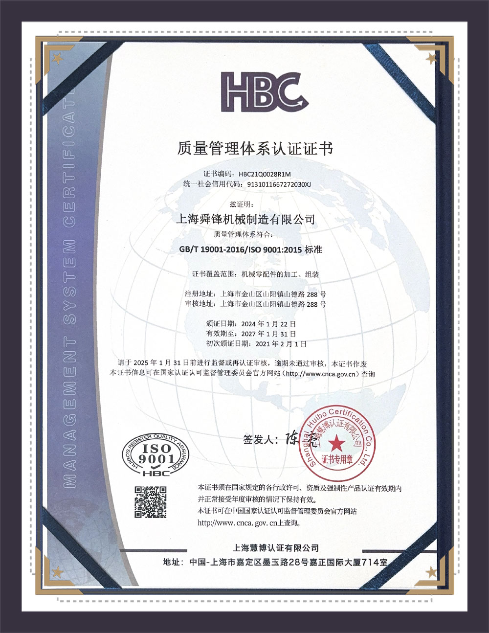
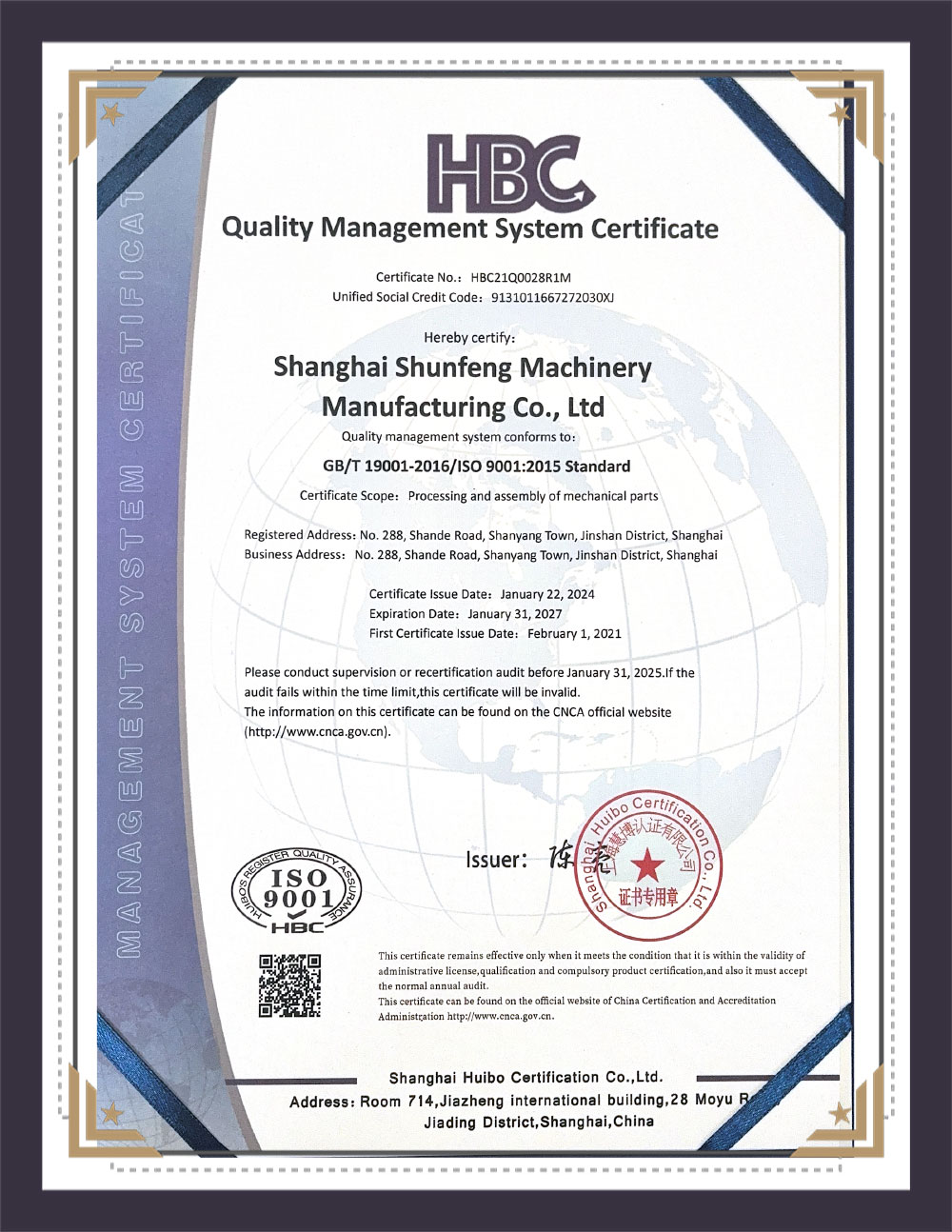
SUNFUN Group applies material certification, dimensional verification, surface finish measurement, and cleanliness inspection to all power device processing equipment component production. Our accredited technology enterprise status supports comprehensive quality systems for semiconductor wafer processing equipment, ensuring consistent component quality and reliable device processing performance.


 English
 日本語
日本語
 عربى
عربى
 中文简体
中文简体