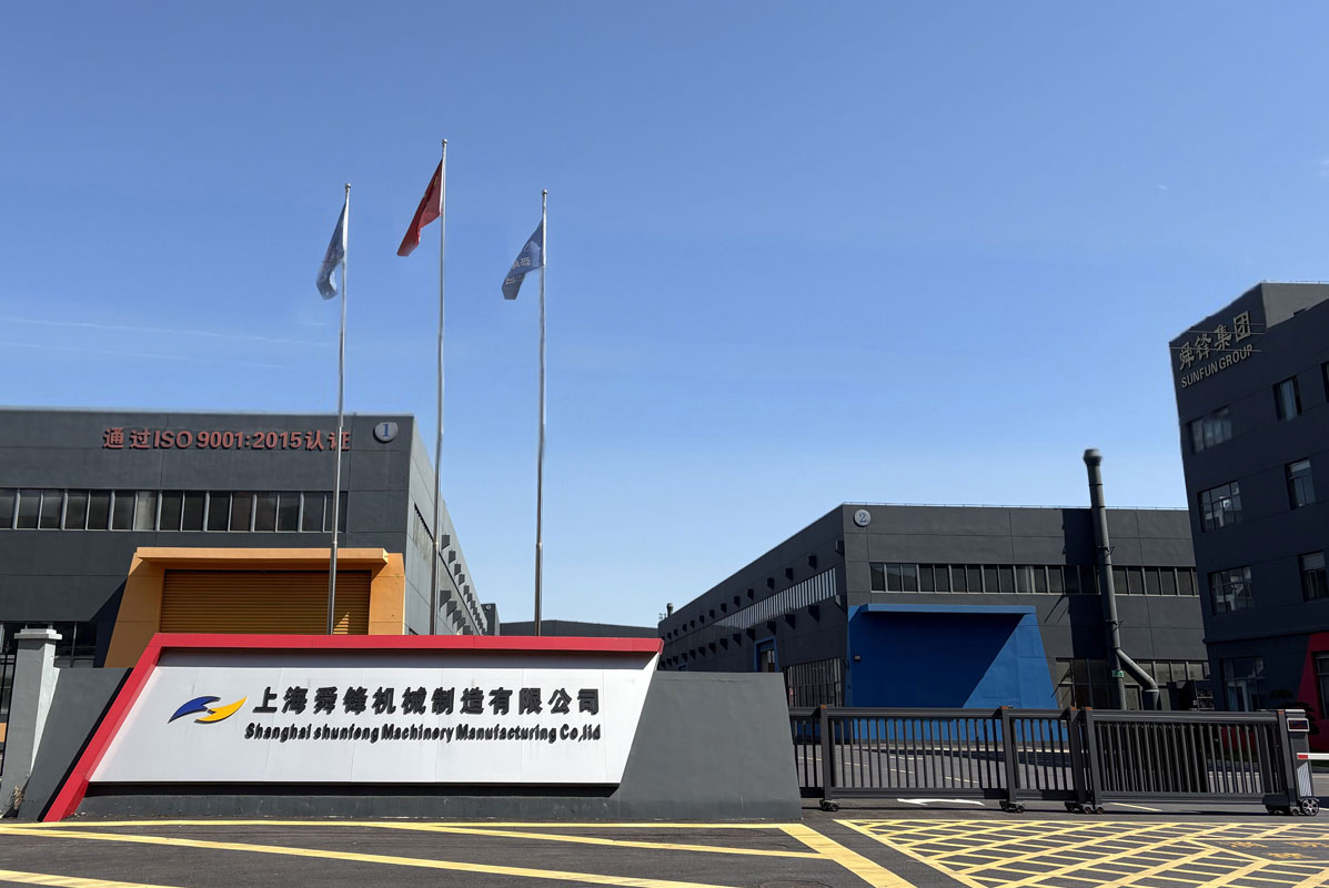
SUNFUN Group specializes in intelligent and sustainable industrial development. Driving quality advancement in manufacturing across China and the globe through technological innovation, we are committed to creating green value for a better human life.
We have deep expertise in smart energy and smart manufacturing, consistently achieving breakthroughs in precision production. Our capabilities range from 0.001-mm precision machining to the manufacture of components weighing from 0.1 grams to 150 tons. We maintain energy consumption within 0.1% and implement fully intelligent process management—all supported by four decades of specialized experience!
Innovation is the foundation of the growth of our group. We have built an open and collaborative innovation ecosystem, partnering with governments, enterprises, universities, and institutions to enable cooperative innovation and shared value, injecting sustained momentum into the industry.<br/>
As an accredited technology enterprise with its own institute and talent academy, SUNFUN has completed more than ten national-level R&D tasks and undertaken major projects commissioned by agencies such as the NDRC, MOST, and MIIT.
For HBM、AI、HPC、Chiplet、2.5D/3D IC、3D NAND
The D2W-TCB bonding equipment is mainly used for high-precision chip interconnection and three-dimensional stacking in the field of advanced packaging. It is targeted at scenarios such as AI computing power, high-performance computing, data centers, and high-end electronics, providing high-precision and high-reliability bonding solutions for high-bandwidth memory(HBM), chip-level heterogeneous integration, and 2.5/3D advanced packaging.
Features
● Meet SEMI S2,F47 Standards
● Fully Automated EFEM
● High Precision Wafer Transfer System
● High Precision Temperature Control
● High Precision Pressure Control
● 8”/12” Compatible
● Pre-bonding at Room Temperature
● High Precision Bonding Intensity Control
● High Precision Alignment
● AVM Unit
● Modular Design, Low Maintenance Cost
● High Throughput